
Course Material
II B.Tech
|
S.No |
Name of the Subject |
|
1 |
|
|
2 |
|
|
3 |
|
|
4 |
|
|
5 |
|
|
6 |
|
|
7 |
|
|
8 |
III B.Tech
|
S.No |
Name of the Subject |
|
1 |
|
|
2 |
|
|
3 |
|
|
4 |
|
|
5 |
|
|
6 |
|
|
7 |
|
|
8 |
|
|
9 |
IV B.Tech
|
S.No |
Name of the Subject |
|
1 |
|
|
2 |
|
|
3 |
|
|
4 |
|
|
5 |
|
|
6 |
|
|
7 |
LAB MANUAL
INNOVATIVE TEACHING LEARNING METHODS
The Contributions made by ECE Department Faculty towards inculcating innovative methods in Teaching and Learning are clearly elucidated both in our Department Records and on the Institute Website for peer review and critique. These methods provide scopes to enhance and reproduction of the same.
For further details click here
Some of our inclusive ways are listed below:
1. Mind Map
2. Flipped Class Room
3. e-Content Delivery
4. Activity based Learning
5. Learning By Doing
6. Digital Library
7. Content Delivery by Video lecture
8. Extension of Ph.D work (Reusability & Reproducibility)
Below are the Short Descriptions on above Innovative means in Teaching and Learning:
1. Mind Map:
A mind map is a diagram used to visually organize information. A mind map is hierarchical and shows relationships among pieces of the whole. It is often created around a single concept, drawn as an image in the center of a blank page, to which associated representations of ideas such as images, words and parts of words are added. Major ideas are connected directly to the central concept, and other ideas branch out from those.
Objectives:
1. To generate, visualize, structure and classify ideas, and as an aid to studying and organizing information, solving problems, making decisions, and writing.
2. To help students with critical and creative thinking and improve their problem-solving ability at the same time.
Outcomes:
1. The study's ability of both students and faculty will get accelerated by improving and enhancing their retention with the combination of photography and information.
2. Problem Solving Ability of students will get improved.
Mind Mapping:
Faculty: Dr.P K Pradhan Associate Prof.
Subject: “Image and computer vision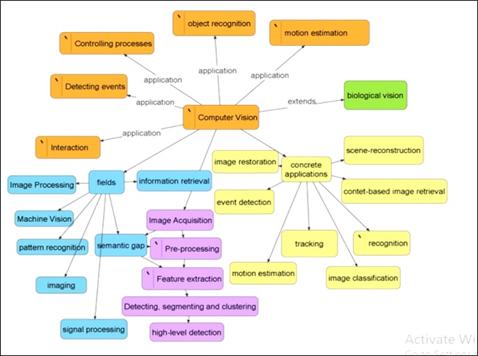
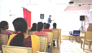
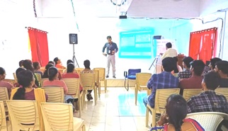
2. Flipped Class Room:
The flipped classroom is a teaching approach where our students get their first exposure to course content before coming to class through readings and video lectures. They then spend in-class time engaging in activities that we’ve designed to promote a deeper understanding of a concept.
Objectives:
1. To promote flexible learning among students.
2. To facilitate increased engagement between students and faculty.
3. To provide prompt and timely feedback to students based on their out of class assessment performance.
Outcomes:
1. Resonate well with those who are high performers and those who tend to underperform.
2. Enhance Faculty interaction with students by scheduled class meetings for dialogue.
Method: Flipped classroom
Name of the Staff: Dr Towheed Sultana
Subject Digital Electronics
Topic Flip Flops
NPTEL Video lecture no 29 and 30 were shared to students to study and to note down any doubts. The same vedio was played in the class and discussed to clear the doubts
Links of Lectures for the topic Flip Flops
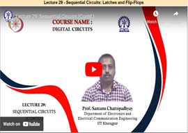
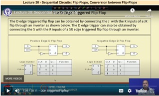
At the end of the class a quiz of 10 questions on the topic Flip Flop was conducted. The performance was amazing.
The activity helped the students do better as it included interactions and discussions which helped them to understand the topic better.
At the end of the class a quiz of 10 questions on the topic Flip Flop was conducted. The performance was amazing.
The activity helped the students do belter as it included interactions and discussions which helped them to understand the topic better.
3. e-Content Delivery
E-Resources Subscriptions links
|
S.No |
E Resource |
Link |
|
1 |
E-Resources Institutional Subscription link in College Website |
|
|
2 |
IEEE(ASPP) |
|
|
3 |
e-Shodh-Sindhu |
|
|
4 |
INFLIBNET–N-LIST (A College component of e-Shodh Sindhu) |
https://nlist.inflibnet.ac.in/ |
|
5 |
National Digital Library of India |
https://ndl.iitkgp.ac.in/ |
|
6 |
Delnet |
|
|
7 |
Swayam Prabha |
https://www.swayamprabha.gov.in/ |
|
8 |
Shodhganga: are servoir of Indian theses@ INFLIBNET |
https://shodhganga.inflibnet.ac.in/ |
|
9 |
Meridian Digital World |
http://34.106.252.76:8087/ |
|
10 |
OPAC |
|
|
11 |
NPTEL |
4. Activity based Learning
The activity method is a technique adopted by a teacher to emphasize his or her method of teaching through activity in which the students participate rigorously and bring about efficient learning experiences. Learning by doing is the main focus of this method. Learning by doing is imperative in successful learning since it is well proved that more the senses are stimulated, the more a person learns and longer he/she retains.
Objectives:
1. To enhance the creative aspect of the experience.
2. To build the student’s self-confidence and to develop understanding through work in their group.
Outcomes:
1. Happy relationships between students and students, teachers and students will be developed.
Method: Activity Based Learning
Name of the Faculty: Mrs. K. Shilpa
Name of the Subject: Signals & Systems
Year & Semester: II Year I Semester
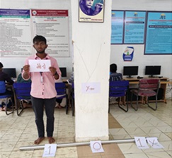
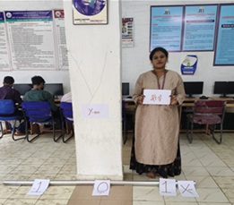
Process: Shifting of impulse function
Shifting of Impulse signal is been explained with an activity, if original signal function of t at 0 on x-axis is been operated with t-1 then it will be shifted to the Right as shown similarly for t+1 operation signal will be shifted to the left as depicted in a picture.
5. Learning by doing:
Department has two dedicated labs for implementing “Learning by doing” methodology. In these labs, students are provided with hands-on training for the better learning experience. Labs and classes are held together to implement “Learning by doing”.
Method: Learning by doing
Name of the Faculty: Ms. Jyothi
Name of the Subject: BEEE
Year & Semester: I Year I Sem
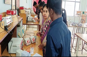
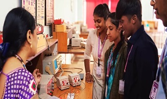
Process: Students are performing the common emitter base configuration characteristics and observing how the operating point on the load line will affect the amplification factor.
6. Digital Library:
JBIET is having a Digital Library facility. It is equipped with the Intel Tidal Data server having storage of 4 TB Capacity. 500 users can access simultaneously.
It is having the following features:
• Tidal Data Server
• Unified Library Server
• NAS
• SAN
• Jukebox
• SATA Disks 1000 GB
• Storage Router
• e-Learning Video Server Streamer
• Mail Server
• Proxy Server
• Print Server
• Server Management Software
• Client Access Manager
• 500 users capacity
7. Content Delivery by Official College Website:
Study materials of the Courses are made available online in our official web site. www.jbiet.edu.in
8. Reproducibility of Ph.D. Work
Ph.D. holders of the department motivate students and staff for brainstorming future ideas on the existing Ph.D. works.
Name of the Faculty: Dr. Anindya Jana
Dept.: Electronics & Communication Engineering
Designation: Professor & Dean- IIIC
Title: Modeling of Nanoscale Devices & Exploring their Applications
Abstract:
Since, the beginning of the seventies, the microelectronics industry has followed Moore’s law, doubling processing power energy in every eighteen months. This performance increase has been achieved by improving the speed and decreasing both the power consumption and size of devices and circuits. Recent advances in crystal growth techniques like fine line lithography, metal organic chemical vapor deposition (MOCVD) and molecular beam epitaxy have made possible the fabrication of low dimensional semiconductor structures. The possibility of realization of high speed devices using such low-dimensional structures has stimulated active research in quasi-low dimensional structures. Continuous evolution in technology over the years has shrunk devices and systems so much that these dimensions are now less than a 1/10th of a micron. The term nano electronics is therefore used instead of microelectronics. The planar silicon metal-oxide semiconductor field-effect transistor (MOSFET) is perhaps the most important invention in the field of micro electronics. MOSFET performance has been improved at a dramatic rate via gate length scaling and is the dominating technology for integrated circuits. For long channel devices, dimensions and supply voltages are scaled by the same factor in order to maintain a constant electric field to achieve the specifications. Modern short channel devices use both the supply voltage and device geometry scaling by different factors. Moore’s prediction has held over the last four decades and will continue as long as the cost of a transistor continues to drop in price.
For more than two decades the rapid progress in complementary metal-oxide-semiconductor (MOS) technology has taken place through the tremendous pace of scaling, leading to an enormous increase in speed and functionality of electronic devices. It is becoming increasingly difficult to meet MOSFET performance gains with reasonable device leakage. Now the gate leakage current constitutes a major part of the power budget of microprocessors. Another critical scaling issue involves the increase of the source-drain resistance resulting from the need for ultra-shallow p-n junctions in the source-drain regions. To keep the source-drain series resistance at a reasonable fraction of the total channel resistance, several alternative MOSFET structures have been proposed, such as non-overlapped gate structures, which do not require ultrashallow source-drain functions or structures with metallic source and drain electrodes to minimize the series resistance. Continuous device performance improvement is possible only through a combination of device scaling, new device structures and material property improvement to its fundamental limits. Retaining the same functional efficiency and achieving further minimization only through device scaling, has become almost impossible for planar CMOS due to some internal physical limitations. However, there have been reports suggesting that the CMOS transistor cannot shrunk beyond certain limits dictated by its operating principle. Over recent years this realization has lead to exploration of possible successor technologies with greater scaling potential such as quantum and single electronics for the next generation VLSI/ULSI circuits.
The single electron tunneling (SET) technology is one of the most promising future technologies to meet the required increase in density, performance and decrease in power dissipation. While the prospect of CMOS devices being completely replaced by SET devices remains to be seen. SET devices and circuits have received tremendous attention in the research community. Hybridization of the SET with complementary MOS technology has attracted much attention in recent years since such integration offers new functionalities, which are very difficult to achieve either by pure CMOS or by pure SET approaches. Consequently, Silicon SETs are appearing to be more promising than metallic SETs for their possible integration with CMOS.
Spintronics is a spin based electronic device technology that combines several characteristics like low power consumption, high operating speed and high integration density, making it financially indispensable in modern electronics. Conventional electronics encode information using the electronic charge. But in Spintronics, the spin of electrons and charge are used together to represent binary data values, rather than charge alone. Because of several distinct features the possibility of developing devices that could be much smaller, consume less electricity and be more powerful for certain types of computation than is possible with system based on electronic charge transport based devices.
In view of the above declarations the candidate wants to study some nano device models and to explore some of their applications.
Session for Faculty Members
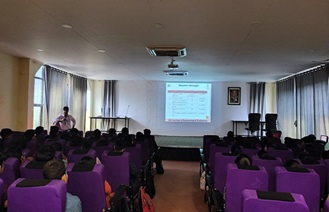
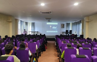
Session for Students